Metal-Electrode Molecular Junction — Au(111)/molecule/Au(111)
The tutorial so far built both the electrodes and the scattering region out of a single 1D carbon chain. The standard problem that the NEGF methodology targeted from the beginning, however, is a molecule sandwiched between two bulk (infinite) metal electrodes. This chapter takes the most thoroughly validated system in the literature — benzenedithiol (BDT) between Au(111) electrodes — as its example, and organizes where the design, structure preparation, and k-sampling of a 3D bulk-electrode system diverge from the 1D chain. The methodological skeleton is unchanged. The scattering region (contact) must include not only the molecule but part of the electrodes as well, must be large enough for screening to complete inside it, and the effect of the semi-infinite electrodes enters through a self-energy constructed recursively from the bulk electrode Green function (the surface Green function recursion is López Sancho et al. 1984). At finite bias, the two electrodes provide the boundary conditions of the electrostatic potential, and the potential profile between them is determined by the SCF — this structure is exactly the same as the C19N device of Chapter 06.
Learning objectives
- Explain the four axes along which a 3D bulk-electrode junction differs from a 1D chain system (electrode dimensionality, transverse periodicity, screening, structural degrees of freedom).
- Design the Au(111) electrode principal layer and the scattering region (molecule + several electrode layers), and judge whether screening is complete.
- Carry out the three structure-preparation steps: fix the bulk lattice → relax the surface slab + molecule → assemble the device.
- Set the k-sampling for the electrode, the device SCF, and TBtrans correctly — especially the placement rule for the TBtrans transverse k block.
- Interpret the of the BDT junction within the off-resonant tunneling picture.
What differs from the 1D chain
| Axis | 1D carbon chain (Chapters 05–09) | Au(111) molecular junction |
|---|---|---|
| Electrode dimensionality | 1D — , are vacuum | 3D bulk — , are periodic too |
| Transverse periodicity | None ( alone suffices) | Present — sampling is mandatory, is a k-average |
| Screening | Slow decay because it is 1D — make the buffer section long | Short because it is a metal (a few Å). Instead, the interface dipole created by interfacial charge transfer means several electrode layers must be included in the scattering region |
| Structural degrees of freedom | Roughly the bond length | Anchoring site (hollow/bridge/top), molecular tilt, adsorption distance — the conductance is sensitive to these |
System design
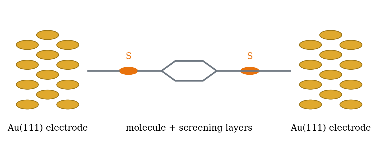
Figure 1. Schematic of a benzenedithiol junction bonded to Au(111) electrodes through thiol (S) anchoring — the scattering region must include, together with the molecule, enough electrode layers for screening to complete. (Conceptual diagram)
Electrode — the Au(111) principal layer
The conditions the electrode must satisfy are exactly the three conditions of Chapter 05. The transport direction is [111], and the literature standard surface cell is 3×3 (9 atoms per layer), which secures the separation between one molecule and its periodic images. In a 3×3 cell the molecule–molecule distance is about 8.8 Å; the literature confirms that for a molecule the size of BDT the interaction between periodic images is small at this setting.
The number of layers must satisfy two conditions simultaneously.
- Preserve the ABC stacking period — stacking along the fcc [111] direction is ABCABC…, so the number of layers in the periodic cell must be a multiple of 3 to avoid creating a stacking fault upon repetition.
- Principal layer condition — judge condition 2 of Chapter 05 (absence of hopping beyond adjacent cells) using the orbital reach. Given the reach of Au DZP orbitals, 3 layers (about 7 Å thick) may be too thin, so 6 layers (about 14 Å) is the safe choice. Early literature calculations (Stokbro et al. 2003) used 3 layers with a shorter basis — check the orbital cutoff radius in your own stdout for your basis and decide (the same procedure as Chapter 05 exercise 2).
Molecule and anchoring — benzenedithiol
BDT () is the standard system treated both by the first generation of single-molecule conductance measurements (Reed et al. 1997) and by the early validation calculations of TranSIESTA (Stokbro et al. 2003). The thiol hydrogen dissociates and the resulting thiolate S bonds to the Au surface; on Au(111) the hollow site (the center above three Au atoms) is reported to be preferred. Since the S–Au bond strength and the conductance change with the anchoring site (hollow/bridge/top) and the molecular tilt, structural degrees of freedom absent in the 1D chain become part of the calculation design. Always state which site was adopted when reporting results.
Scattering region — molecule + 3–4 Au layers on each side
The scattering region of the device does not end with the molecule. The electrostatic perturbation created by charge transfer and the dipole at the S–Au interface must finish decaying inside the device to meet the electrode self-energy smoothly. Metallic screening is short, so 3–4 Au layers from the interface are generally sufficient, but this is a matter for judgment, not assumption — check whether the planar-averaged potential of the boundary layers and the layer-resolved PDOS match the bulk electrode values. Apply criteria 1 and 2 of scattering region convergence verbatim for the judgment criteria and the length-series procedure.
Structure preparation procedure
The structure is fixed in three steps. The VASP → SIESTA cross-validation flow laid out in Chapter 03 (transfer of lattice and coordinates, comparison of band shapes, comparison of relative energy ordering — never compare absolute energies) is the standard here as well.
- Fix the bulk Au lattice constant — converge the lattice constant of fcc Au with VASP and with SIESTA (PBE/DZP) separately and confirm that they agree. Since every subsequent structure (electrode cell, slab, device) stands on this value, criterion 3 of scattering region convergence (fix the electrode lattice by bulk-only relaxation) is the starting point.
- Relax the surface slab + molecule — with the fixed lattice, build an Au(111) slab (4–6 layers, vacuum along the surface normal), place BDT on it, and relax. Here, fix the inner electrode layers at their bulk positions and move only the molecule and the interfacial Au (the top 1–2 layers). If you release the structure all the way down through the slab, the atomic arrangement will not match the electrode replica region when the device is assembled. Apply the same constraint with
Geometry.Constraintsin SIESTA and with Selective dynamics in the VASP POSCAR. - Assemble the device — place the relaxed interface structure (molecule + interfacial Au layers) at the center and attach electrode cells, replicated verbatim, at both ends. The electrode replica regions must be completely identical in atomic species, spacing, and arrangement to the electrode cell (exactly the boundary condition of Chapter 06). Along the transport direction (), atoms run continuously from the left electrode to the right electrode, so there is no vacuum — and the transverse directions have no vacuum either, being 3×3 surface periodic. Unlike the 1D example, no vacuum enters anywhere in the device cell.
# Slab atom order: sorting from bottom (electrode side) -> top (molecule side) keeps range specification simple
%block Geometry.Constraints
  atom [1 -- 27]        # Fix the bottom 3 Au layers (3x3x3 = 27 atoms) at bulk positions
%endblock Geometry.Constraints
k-sampling — the decisive point of divergence from 1D
In the 1D example the transverse directions were vacuum, so there was a single k-point, . In a 3D bulk electrode the transverse directions are genuinely periodic, so sampling enters every stage of the calculation.
| Calculation | k-grid (example) | Rationale |
|---|---|---|
| Bulk Au / electrode | Transverse periodicity + integration of metallic bands along the transport direction. Transverse should be at least as dense as the device | |
| Slab + molecule relax | Surface slab — the vacuum direction is 1 | |
| Device TranSIESTA SCF | Transport-direction k is 1 — the electrode self-energy handles the open boundary (same logic as Chapter 06) | |
| TBtrans | The average is part of the result for — denser than the SCF, convergence check mandatory |
To make the TBtrans transverse k dense, %block TBT.kgrid_Monkhorst_Pack must be placed at the very end of input.fdf. If you put this block inside TBtrans.fdf, the transport-direction k is automatically reduced to 1 and the intended grid is not applied (Chapter 07 pitfall 2). In the 1D example the k-grid was the single point, so this rule never surfaced; in a bulk-electrode system, violating this placement rule breaks k convergence without any warning — the decisive difference from 1D.
%block TBT.kgrid_Monkhorst_Pack
  10   0   0    0.0
   0  10   0    0.0
   0   0   1    0.0
%endblock TBT.kgrid_Monkhorst_Pack
fdf skeleton
Rather than listing all coordinates, only a skeleton focused on how to construct the input is shown. The lattice numbers are derived from the fixed by the bulk relaxation — surface lattice constant , interlayer spacing (the numbers below are an example based on Å).
SystemName   Au(111) electrode, 3x3 surface cell x 6 layers
SystemLabel  Electrode

NumberOfAtoms    54            # 6 layers x 9 atoms, 2 periods of ABC stacking
NumberOfSpecies   1
%block ChemicalSpeciesLabel
  1  79  Au
%endblock ChemicalSpeciesLabel

LatticeConstant 1.0 Ang
%block LatticeVectors
   8.825   0.000   0.000       # 3 x a_surf
  -4.412   7.643   0.000       # hexagonal surface lattice (120 deg)
   0.000   0.000  14.412       # 6 layers x d_111 -- transport direction, no vacuum
%endblock LatticeVectors

# Coordinates: generated from the bulk lattice with ABC stacking. The electrode is not relaxed (ideal crystal).

PAO.BasisSize    DZP
XC.Functional    GGA
XC.Authors       PBE
MeshCutoff       300. Ry

%block kgrid_Monkhorst_Pack
   8   0   0    0.0
   0   8   0    0.0
   0   0  32    0.0
%endblock kgrid_Monkhorst_Pack

SCF.DM.Tolerance   1.0d-8
TS.HS.Save         T           # save Electrode.TSHS
The device TS.fdf has the same block structure as the one in Chapter 06. The only things that change are the electrode TSHS path and the atom ranges that electrode-position points to (54 atoms per electrode replica region).
%block TS.Elecs
  Left
  Right
%endblock TS.Elecs

%block TS.Elec.Left
  HS ../01_electrode_au/Electrode.TSHS
  chemical-potential Left
  semi-inf-direction -a3
  electrode-position 1          # electrode replica region starting from device atom 1
%endblock TS.Elec.Left

%block TS.Elec.Right
  HS ../01_electrode_au/Electrode.TSHS
  chemical-potential Right
  semi-inf-direction +a3
  electrode-position end -1     # electrode replica region ending at the last atom
%endblock TS.Elec.Right
The chemical-potential and contour blocks, the DM.UseSaveDM/TS.HS.Save/Write.DM save flags, and the bias-chain rules (Chapter 09) are all the same as in the 1D example. The condition that basis, functional, and MeshCutoff must be identical in the electrode and the device (Chapter 05) also holds unchanged.
Expected result — off-resonant tunneling
The of a BDT junction looks entirely different from the integer plateaus of the 1D chain.
- lies inside the molecule's HOMO–LUMO gap. Inside the gap, conduction proceeds only by tunneling without resonance, so — a gentle valley rather than a plateau.
- Below appear the HOMO (and states originating from the S–Au bond), and above it the LUMO resonance peak. BDT is known as a HOMO-conducting system, with the HOMO-side resonance closer to .
- That the of a semi-local functional (PBE) overestimates the experimental conductance is a trend repeatedly confirmed in the literature; its cause (level-alignment error) and its correction are the subject of Chapter 11. Because the electrodes are planar metals, this is also a system to which the image-charge correction () — undefined for the 1D chain — can be applied, another connection to Chapter 11.
- Use eigenchannel decomposition (Chapter 10) to check whether the of the dominant channel passes through the S–Au anchoring bond. Since changing the anchoring site changes the channel wavefunction and together, the effect of structural degrees of freedom on the conductance can be diagnosed at the channel level.
Exercises
- For electrode thicknesses of 3 and 6 layers, compute the minimum distance between an atom in cell and an atom in cell in units of , compare it with the Au DZP orbital cutoff (found in the electrode calculation stdout), and judge the principal layer condition — this is the Au version of Chapter 05 exercise 1.
- Design a series that increases the Au in the scattering region to 2/3/4 layers per interface (keeping electrode-cell units). Plan which deliverables (boundary-layer potential, PDOS, overlay) you will use to judge the completion of screening.
- Design a convergence test that overlays while changing the TBtrans transverse k to , , and . Explain where the
TBT.kgrid_Monkhorst_Packblock must be placed and what symptom reveals a wrong placement.
References
- M. Brandbyge, J.-L. Mozos, P. Ordejón, J. Taylor, and K. Stokbro, "Density-functional method for nonequilibrium electron transport", Phys. Rev. B 65, 165401 (2002). DOI 10.1103/PhysRevB.65.165401
- K. Stokbro, J. Taylor, M. Brandbyge, J.-L. Mozos, and P. Ordejón, "Theoretical study of the nonlinear conductance of di-thiol benzene coupled to Au(111) surfaces via thiol and thiolate bonds", Comput. Mater. Sci. 27, 151 (2003). DOI 10.1016/S0927-0256(02)00439-1
- M. A. Reed, C. Zhou, C. J. Muller, T. P. Burgin, and J. M. Tour, "Conductance of a Molecular Junction", Science 278, 252 (1997). DOI 10.1126/science.278.5336.252
- M. P. López Sancho, J. M. López Sancho, and J. Rubio, "Highly convergent schemes for the calculation of bulk and surface Green functions", J. Phys. F: Met. Phys. 15, 851 (1985); the original paper on the recursive algorithm is J. Phys. F 14, 1205 (1984). DOI 10.1088/0305-4608/14/5/016