00. Overview of Quantum Transport — From Ohm to Landauer
This chapter builds the conceptual backbone for the question that runs through the entire tutorial — "how does current flow in a nanoscale device?" There are no calculations yet. We examine why Ohm's law breaks down at the nanoscale, what the Landauer picture that replaces it looks like, and what physical quantity the transmission function — which every later chapter will compute — actually is. Since this is a theory chapter, it contains no input files or run sections; it is organized as theory → key summary → exercises.
Learning objectives
- Explain, from the viewpoint of the scattering length (mean free path), why Ohm's law fails at the nanoscale.
- Understand that in the ballistic limit the resistance does not vanish but saturates at a finite value set by the conductance quantum .
- Learn to read a nanoscale device through an energy level diagram (contact–channel–Fermi level).
- Derive, in the single-level model, how current arises from the competition between the Fermi functions and of the two electrodes.
- Grasp how the transmission function and the Landauer formula generalize this picture.
1. The limits of Ohm's law at the nanoscale
The resistance of a macroscopic conductor is described by Ohm's law.
Here is the resistivity, the length, and the cross-sectional area. Let us extrapolate this formula directly to the nanoscale. For a piece of copper with cross section and length , inserting gives
However, the resistance of real nanoscale devices deviates strongly from this extrapolation. In the extreme case of an atomic-scale conductor with a single conduction channel (an atomic chain, a single-molecule junction), the resistance never drops below about , no matter how perfect the contacts are made.
This does not mean Ohm's law is wrong. The proportionality rests on the assumption that electrons undergo numerous scattering events while traversing the conductor. In a metal at room temperature the electron mean free path is on the order of tens of nm, so when the length shrinks to about 10 nm, electrons pass through the conductor with almost no scattering. This regime is called ballistic transport, and here the resistance arises not inside the conductor but at the contact (interface) between the conductor and the electrodes.
2. The ballistic limit and the conductance quantum
The maximum conductance that a single perfect one-dimensional conduction channel with no scattering can have is a universal constant set by quantum mechanics.
The factor of 2 comes from spin degeneracy. If a conductor has conduction channels (modes), the ballistic-limit conductance is and the resistance saturates at . In other words, no matter how short the conductor is made, the resistance never reaches zero; this residual resistance is a contact resistance arising from the "bottleneck" between the electrodes (reservoirs), which have infinitely many modes, and the channel, which has finitely many. The staircase-like variation of the conductance in units of observed in quantum point contact experiments is direct evidence for this picture (van Wees et al., Phys. Rev. Lett. 60, 848 (1988)).
The example system of this tutorial, the 1D carbon chain (cumulene), has two degenerate channels near the Fermi level, so the ballistic conductance of a perfect chain is and the lower bound on the resistance is about . In later chapters you will verify this value by direct calculation.
3. The energy level diagram — contacts, channel, and Fermi level
The first tool for treating a nanoscale device atomistically is the energy level diagram. We divide the device into three parts.
- Contacts — the large electrodes attached at both ends of the device. They act as electron reservoirs, and their interiors are always assumed to be in thermal equilibrium.
- Channel — the nano region through which electrons actually pass. Because it is small, its energy levels are either discrete (a molecule) or form a quasi-continuous spectrum with narrow level spacing (a nanowire).
- Fermi level — the upper energy bound up to which electrons fill the electrodes and the channel in equilibrium. At absolute zero, all levels below are filled and all above are empty. At finite temperature, the Fermi–Dirac distribution
gives the occupation probability.
In equilibrium, with no applied voltage, both electrodes and the channel share a single common , and the electron flow to the left exactly cancels the flow to the right, so the net current is zero. To drive a current, this balance must be broken.
4. The single-level model — why does current flow?
As the simplest device, consider a channel with only a single energy level () sandwiched between two electrodes. Including spin, this level can hold up to 2 electrons.
Equilibrium. The average occupation of the level is determined by the Fermi function.
Non-equilibrium. Applying a voltage splits the chemical potentials of the two electrodes.
Now the left electrode tries to set the occupation of the level to , while the right electrode tries to set it to . If the level lies in the bias window between the two chemical potentials, then and — the left keeps trying to fill it and the right keeps trying to empty it. This never-ending tug of war is the current.
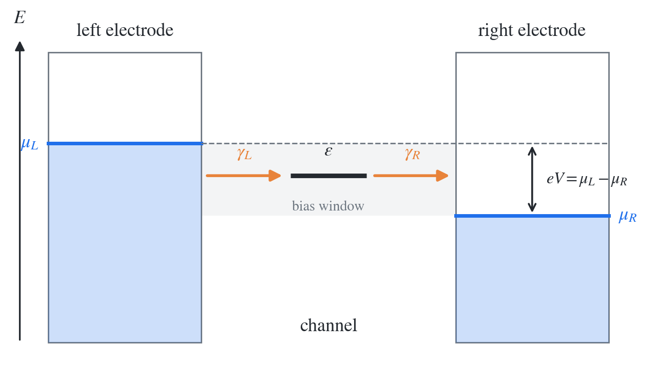
Figure 1. Energy level diagram of the single-level model (schematic) — when the level lies within the bias window (), the left electrode tries to fill it at rate and the right electrode tries to empty it at rate ; this competition is the current.
Let us quantify this. Denoting the electron exchange rate between the level and electrode as (where is the coupling strength in energy units), the time evolution of the occupation is
and in steady state () we obtain
(Datta [1], Ch. 1). What this equation says is the core of this chapter.
- The current is proportional to , i.e., the competition between the two electrodes trying to fill the level differently. If the level lies outside the bias window, and there is no current.
- The magnitude of the current is limited by a harmonic-mean-like combination of the level–electrode couplings . No matter how strong one coupling is, if the other is weak, that bottleneck sets the current.
- The coupling simultaneously determines the lifetime of the level and its energy broadening. A level connected to an open system is no longer an infinitely sharp function; it spreads into a Lorentzian of width . This broadening reappears in Chapter 04 as the imaginary part of the self-energy.
5. Generalization to the transmission function
A real device has not a single level but a continuous spectrum and multiple conduction channels. Generalizing the single-level model, the transmission function — the probability that an electron of energy passes from the left electrode to the right electrode — comes to contain all the transport information of the device, and the current is written with the Landauer formula.
The only interval that effectively contributes to the integral is the bias window where . In the linear-response limit (small ),
so the conductance is determined solely by the transmission at the Fermi level. takes values between 0 and the number of channels ; a perfect ballistic conductor has , while a tunneling junction has .
The rest of this tutorial is, in the end, the story of computing from first principles. Chapter 04 establishes the NEGF formalism that expresses in terms of Green's functions, Chapter 07 extracts for real systems with TBtrans, and Chapter 08 computes I–V curves with the Landauer integral above.
Key summary
| Concept | Content |
|---|---|
| Limits of Ohm's law | applies only to macroscopic conductors with abundant scattering. If is shorter than the mean free path, the regime is ballistic |
| Conductance quantum | , minimum resistance per channel |
| Contact resistance | The residual resistance in the ballistic limit arises not inside the conductor but from the mode bottleneck at the electrode–channel boundary |
| Origin of current | Competition of the two electrodes' Fermi functions: ; only levels inside the bias window contribute |
| Broadening | The coupling to the electrodes spreads the level into a Lorentzian of width () |
| Landauer formula | ; in linear response |
Exercises
-
Ohm extrapolation vs. the quantum lower bound. The gap between the copper-piece example in the text () and the single-channel lower bound spans a full 6 orders of magnitude. Resolve this gap qualitatively by using the fact that a conductor with a cross section actually has a large number of conduction channels. Discuss how the number of channels depends on the cross-sectional area and the Fermi wavelength .
-
Current in the single-level model. Derive the expressions for and directly from the steady-state condition in the text. For symmetric coupling and a level fully inside the bias window so that , compute the current. (; the answer is )
-
Recovering from the Landauer formula. Apply the Landauer integral at absolute zero to a perfect single channel with and show that , i.e., ; convert to resistance and confirm .
Ref: Datta [1], Ch. 1; B. J. van Wees et al., Phys. Rev. Lett. 60, 848 (1988).